鑫景福致力于满足“高品质”PCBA订购单需求。


Seven Tips for Avoiding ElectromagnetIC Problems in PCB Design
electromagnetic compatibility and related electromagnetic interference have always required system design engineers to be vigilant, especially in the current situation of shrinking world economy, PCB board design and component packaging as well as OEM requirements for high-speed systems are a headache for PCB layout and design engineers EMC is closely related to this generation, spreading and receiving electromagnetic energy, and EMC is in PCB design Electromagnetic energy comes from a variety of sources mixed together. In summary, special attention must be paid to ensure that different circuits, traces, through-hole, and PCB data work together, and that various signals are compatible and do not interfere with each other Electromagnetic interference, on the other hand, is a destructive effect produced by EMC or unwanted electromagnetic energy In this electromagnetic environment, PCB designers must ensure that the generation of electromagnetic energy is reduced to minimize interference
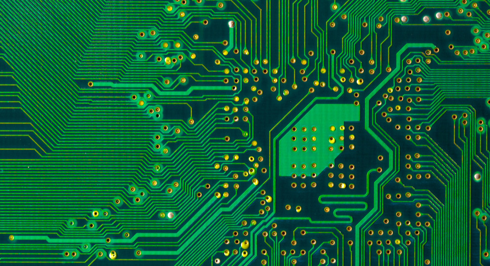
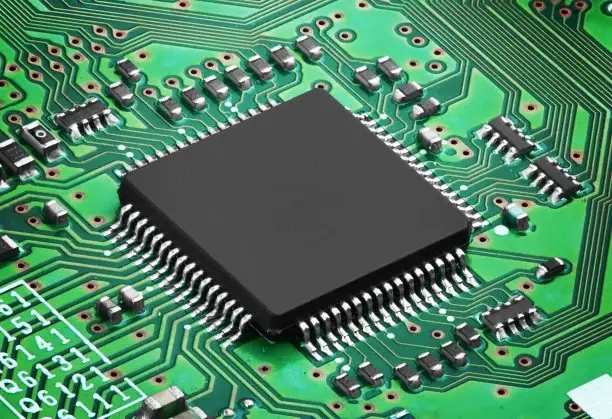
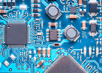
PCB board

Here are 7 tips for avoiding electromagnetic problems PCB design:
Tip 1: Ground the PCB
An important method to reduce EMI is to design the grounding plane of PCB. The first step is to make the grounding area within the total area of PCB board as large as possible, which can reduce emission, crosstalk and noise. Special care must be taken when connecting each component to the ground point or ground plane, otherwise the neutralization effect of a reliable ground plane cannot be fully utilized. The particularly complex PCB design has several stable voltages. Ideally, each reference voltage has its own ground plane. However, if there are too many grounding planes, the manufacturing cost of PCB will be increased, which will make the price too high. The compromise is to use grounding planes at three to five different locations, each of which can contain multiple grounding sections. This not only controls the manufacturing cost of the circuit board, but also reduces EMI and EMC. If you want to keep EMC SMAll, a low impedance grounded system is very important. In a multilayer PCB, it is better to use a solid ground plane rather than a copper balance block or a dispersed ground plane because it has low impedance, provides a current path, and is a good source of reverse signals. In order to solve the EMC problem in multilayer PCB, it is better to use solid grounding plane rather than copper theft or dispersed grounding plane. The length of time it takes for the signal to return to the ground is also important. The time of signal in and out of the source must be comparable, otherwise, when the radiated energy becomes a part of EMI, a phenomenon SIMilar to the antenna will occur. In addition, the trace of the current transmitted from the signal source should be as short as possible. If the length of the source and return paths are not equal, there will be ground rebound, which will also generate EMI. If the timing of the signal entering and leaving the source is not synchronized, a phenomenon similar to the antenna will occur, radiating energy and causing EMI.
Tip 2: Differentiate EMI
Due to different EMI, a good EMC design rule is to separate analog and digital circuits. Analogue circuits with high current intensity or current shall be far away from high-speed tracks or switching signals. If possible, they should be protected by an earth signal. On a multilayer PCB, the analog trace should be routed on one ground plane, and the switch or high-speed trace should be located on another ground plane. Recall that signals with different characteristics are separated. Low pass filter can sometimes be used to remove high-frequency noise coupLED with the surrounding track. The filter suppresses noise and returns a steady current. It is important to separate the ground plane of analog and digital signals. Since analog circuits and digital circuits have their unique characteristics, it is important to separate them. Digital signals shall have digital grounding, and analog signals shall terminate in analog grounding. In digital circuit design, experienced PCB layout and design engineers pay special attention to high-speed signals and clocks. At high speeds, signals and clocks should be as short as possible and adjacent to the ground plane, which, as previously described, keeps crosstalk, noise and radiation under control. Digital signals should also be away from the power plane. If the distance is close, noise or induction will be generated, which will weaken the signal.
Tip 3: Crosstalk and trajectory are important
Traces are particularly important to ensure proper current flow. If the current comes from an oscillator or other similar device, it is particularly important to keep the current separate from the ground plane or not to parallelize the current with another trace. Two parallel high-speed signals generate EMC and EMI, especially crosstalk. The resistance path must be kept short and the return path must be as short as possible. The return path trace should be the same length as the transfer trace. For EMI, one is called "aggressor trace", and the other is "victim trace". Due to the existence of electromagnetic field, the coupling of inductance and capacitance will affect the "victim" track and generate forward and reverse currents on the "victim" track. In this case, ripples are generated in a stable environment where the transmission and reception lengths of signals are almost equal. In a well balanced environment with a stable trajectory, the induced currents should cancel each other to eliminate crosstalk. However, we live in an imperfect world, and such things will not happen. Recall that our goal must be to keep crosstalk of all trajectories to a very small level. If the width between parallel traces is twice the trace width, the crosstalk effect can be minimized. For example, if the trace width is 5 mils, the small distance between two parallel traces should be 10 mils or more. With the continuous emergence of new materials and components, PCB designers must continue to deal with electromagnetic compatibility and interference problems.
Tip 4: Decoupling capacitors
Decoupling capacitors can reduce the adverse effects of crosstalk and should be placed between the power supply and grounding pins of the equipment to ensure low AC impedance and reduce noise and crosstalk. In order to achieve low impedance over a wide frequency range, multiple decoupling capacitors should be used. Decoupling capacitors are used around the ball grid array to reduce crosstalk. An important rule of thumb for placing decoupling capacitors is to place small value capacitors as close to the equipment as possible to reduce the inductance impact on the trace. The specific capacitor shall be as close as possible to the power supply pin or power trace of the device, and the bonding pad of the capacitor shall be directly connected to the through hole or grounding plane. If the trace is long, use multiple through holes so that the grounding impedance is low.
Tip 5: Avoid 90 degree angles
To reduce EMI, avoid traces, through holes, and other components that form a 90 ° angle, because right angles generate radiation. In this corner, the capacitance will be added, and the characteristic impedance will change, which will cause reflection, and then lead to EMI. To avoid a 90 ° angle, the trace should be routed to at least two 45 ° angles.
Tip 6: Use through-hole with care
In almost all PCB board layouts, through holes must be used to provide conductive connections between different layers. PCB layout engineers need to be very careful, because through holes generate inductance and capacitance. In some cases, they also generate reflections because the characteristic impedance changes when a through-hole is formed in the trace. In addition, remember that the through-hole will increase the trace length and need to be matched. In the case of differential traces, through holes should be avoided as much as possible. If unavoidable, through holes should be used in both traces to compensate for delays in signals and return paths.
Tip 7: Cables and physical masks
The cable carrying digital circuit and analog current will generate parasitic capacitance and inductance, resulting in many EMC related problems If twisted pair cables are used, the coupling level is kept low and the magnetic field generated is eliminated For high-frequency signals, shielded cables must be used to eliminate EMI interference with the front and background Physical mask is used to package the whole or part of the system with metal package to prevent EMI from entering the Circuit PCB The mask is similar to a closed grounding conductive container, reducing the size of antenna loop and absorbing EMI

抖音二维码

Q Q二维码

微信二维码
点击
然后
联系
然后
联系
电话热线
13410863085Q Q

微信

- 邮箱