鑫景福致力于满足“高品质”PCBA订购单需求。


The surface treatment methods used in Pcb factory proofing are different, and each surface treatment method has its unique characteristICs. Take chEMIcal silver as an example, its manufacturing process is extremely SIMple, and it is recommended to be used in lead-free welding and SMT, especially for fine lines. The most important thing is to use chemical silver for surface treatment, which will greatly reduce the overall cost and lower the cost. The following is a brief introduction of several common surface treatment methods for PCB board proofing.

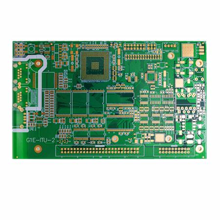
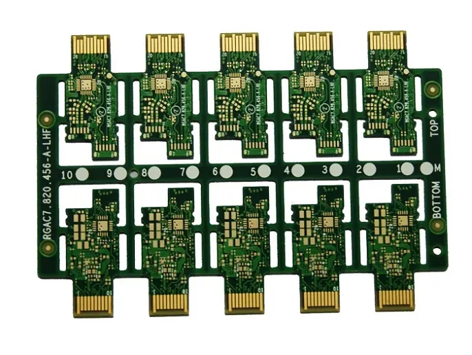
PCB factory proofing
1. HASL hot air leveling (commonly known as tin spraying)
Tin spraying is a common method in the early stage of PCB board proofing. Now it is divided into lead tin spraying and lead-free tin spraying. Advantages of tin spraying: After the PCB is completed, the copper surface is completely wetted (completely covered with tin before welding), which is suitable for lead-free welding. The process is mature and the cost is low, which is suitable for visual inspection and electrical testing. It is also one of the high-quality and reliable PCB board proofing methods.
2. Chemical nickel gold (ENIG)
Nickel plated gold is a widely used surface treatment process for PCB plate proofing. Remember that nickel layer is a nickel phOSPhorus alloy layer, which can be divided into high phosphorus nickel and medium phosphorus nickel according to phosphorus content. Their applications are different, and their differences will not be introduced here. Advantages of nickel gold: suitable for lead-free welding; The surface is very flat, suitable for SMT, electrical testing, switch contact design, aluminum wire binding, thick plate, and strong resistance to environmental attacks.
3. Nickel gold electroplating
Electroplated nickel gold is divided into "hard gold" and "soft gold". Hard gold (such as gold cobalt alloy) is often used on gold finger (contact connection design), and soft gold is pure gold. Electroplated nickel gold is widely used on IC carrier plates (such as PBGA) and is mainly suitable for binding gold wire and copper wire. However, the IC carrier plate is suitable for electroplating, and the binding gold finger area needs additional conductor wires for electroplating. Advantages of nickel gold plated PCB: suitable for contact switch design and gold wire binding; Suitable for electrical testing
4. Nickel palladium (ENEPIG)
Nickel palladium is now gradually beginning to be used in the field of PCB board proofing, and was previously used more in semiconductors. Suitable for binding with gold and aluminum wires. Advantages of using nickel palladium PCB board for proofing: It is applicable to IC carrier board, suitable for gold wire binding and aluminum wire binding. Suitable for lead-free welding; Compared with ENIG, there is no nickel corrosion (black disc) problem; The cost is cheaper than ENIG and electronickel gold, and it is suitable for a variety of surface treatment processes and stored on the board


抖音二维码

Q Q二维码

微信二维码
点击
然后
联系
然后
联系
电话热线
13410863085Q Q

微信

- 邮箱