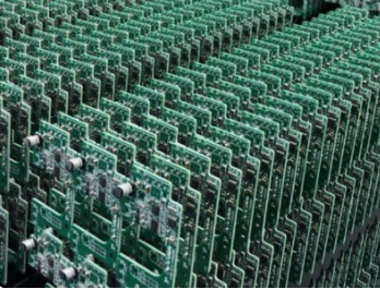
鑫景福致力于满足“高品质”PCBA订购单需求。


The stack design of PCB is not a SIMple stack of layers. The arrangement of layers is the key, whICh is closely related to the arrangement and trend of signals. Compared with ordinary pcbs, the design of multilayer boards adds necessary signal routing layers, and the most important thing is to arrange independent power supply and layers (copper layer). In the high-speed digital circuit system, the advantages of using power supply and stratum to replace the previous power supply and ground bus mainly lie in:

1) It provides a stable reference voltage for digital signal transformation.
2) Evenly add the power supply to each logic device at the same time.
3) Effectively suppress crosstalk between signals.
The reason is that using a large area of copper as the power supply and stratum greatly reduces the resistance between the power supply and the ground, making the voltage on the power supply layer even and stable, and ensuring that each signal line has a very close horizon correspondence, which also reduces the characteristic impedance of the signal line and effectively reduces crosstalk. Therefore, for some high-end high-speed circuit designs, it has been explicitly stipulated that a 6-layer (or more) stacking scheme must be used, such as Intel's requirements for PC133 memory module PCB. This is mainly due to the fact that Multilayer boards are obviously superior to low layer PCBs in terms of electrical characteristics, electromagnetic radiation suppression, and even physical and mechanical damage resistance.
In general, the stack design shall follow the following principles: meet the characteristic impedance requirements of the signal; Meet the principle of signal loop minimization; Meet the requirements of minimizing signal interference in PCB; Meet the principle of symmetry. Specifically, the following aspects should be paid attention to when designing multilayer boards:
1) A signal layer should be adjacent to a copper coating layer, and the signal layer and copper coating layer should be placed at intervals. It is better that each signal layer can be closely adjacent to at least one copper coating layer. The signal layer should be closely coupLED with the adjacent copper layer (that is, the medium thickness between the signal layer and the adjacent copper layer is very SMAll).
2) Power copper coating and ground copper coating shall be tightly coupled and located in the middle of the stack. Shortening the distance between the power supply and the stratum is conducive to the stability of the power supply and the reduction of EMI. The signal layer shall not be sandwiched between the power layer and the stratum as far as possible. The close proximity of the power plane and the ground plane is like forming a flat plate capacitor. The closer the two planes are, the greater the capacitance value. The main function of the capacitor is to provide a low impedance return path for high-frequency noise (such as switching noise, etc.), so that the power input of the receiving device has a smaller ripple and enhances the performance of the receiver itself.
3) In the case of high speed, redundant layers can be added to isolate the signal layer. Multiple copper layers can effectively reduce the impedance of PCB and reduce common mode EMI. However, it is recommended not to add more power layers for isolation, which may cause unnecessary noise interference.
4) The high-speed signal in the system should be in the inner layer and between two copper coatings, so that the two copper coatings can provide shielding for these high-speed signals, and limit the radiation of these signals to two copper coating areas.
5) Give priority to the transmission line model of high-speed signals and clock signals, design a complete reference plane for these signals, and try to avoid cross plane segmentation to control the characteristic impedance and ensure the integrity of the signal return path.
6) Two signal layers are adjacent. For boards with high-speed signals, the ideal lamination is to design a complete reference plane for each high-speed signal layer, but in practice, we always need to make a trade-off between the number of PCB layers and PCB cost. In this case, it is unavoidable that two signal layers are adjacent. The current practice is to increase the distance between the two signal layers and make the routing of the two layers as vertical as possible to avoid signal crosstalk between layers.
7) It is better to lay copper layers in pairs. For example, two or five layers or three or four layers of the Six layer board should be laid with copper together. This is to consider the requirements of balanced structure in the process, because the unbalanced copper layer may lead to PCB warping and deformation.
8) The sub surface (i.e. the layer close to the surface) is designed as a stratum, which is conducive to reducing EMI.
9) According to pcb device density and pin density, the required number of signal layers is estimated to determine the total number of layers.
The board structure is a very important factor to determine the EMC performance of the system. A good board structure plays a good role in suppressing radiation in PCB. In the current common high-speed circuit system, multilayer boards are mostly used instead of single panel and double-sided boards. The following is a brief description of the structural design of the four layer, six layer, eight layer and ten layer boards.
Four layer Board Design
Generally speaking, for more complex high-speed circuits, it is better not to use a four layer board because it has a number of unstable factors, both physically and electrically. If a four layer board design is necessary, it can be set as: power signal signal ground. There is also a better solution: the outer two layers are both strata, and the inner two layers are power and signal lines. This scheme is the best lamination scheme for four layer board design, which has an excellent inhibition effect on EMI and is also very beneficial to reduce the impedance of signal lines. However, it is difficult for boards with large wiring density because of small wiring space.
Six layer board design
At present, many circuit boards adopt the six layer board technology, such as the design of memory module PCB, most of which adopt the six layer board (10 layers may be used for high-capacity memory modules). The most conventional six layer laminate is arranged as follows: signal ground signal signal power signal. From the point of view of impedance control, this arrangement is reasonable, but because the power supply is far from the ground plane, the radiation effect on small common mode EMI is not very good. If the copper coating area is placed on layers 3 and 4, it will cause problems such as poor signal impedance control and strong differential mode EMI. Another solution is to add a ground plane layer. The layout is: signal ground signal power ground signal. In this way, the environment required for high-speed signal integrity design can be achieved from the perspective of impedance control or EMI reduction. However, the disadvantage is that the layers are stacked unevenly. The third layer is the signal wiring layer, but the corresponding fourth layer is the power supply layer with a large area of copper coating. This may encounter a problem in PCB process manufacturing. In the design, copper can be applied to all blank areas of the third layer to achieve an approximate balanced structure.
Eight layer board design
Most of the eight ply boards used today are designed to improve the signal quality of the six ply board. Compared with the six layer board, the eight layer board does not increase the signal routing layer, but has two more copper layers, so it can optimize the EMC performance of the system.
Ten layer board design
The insulation medium layer of the ten layer PCB is very thin, and the signal layer can be close to the ground plane, so that the impedance change between layers can be well controlled. Generally, as long as there is no serious stacking design error, designers can easily complete high-quality high-speed circuit board design. If the routing is very complex and requires more routing layers, we can set the stack as: signal signal ground signal signal signal signal power signal. Of course, this situation is not ideal. We require signal routing to be completed in a few layers, but use redundant layers to isolate other signal layers. Therefore, the more common stacking scheme is: signal ground signal signal power ground signal ground signal signal ground signal. It can be seen that three ground plane layers are used here, and only one layer of power supply is used (we only consider the case of single power supply). This is because, although the effect of the power layer on impedance control is the same as that of the ground layer, the voltage on the power layer is greatly disturbed, there are many higher-order harmonics, and the EMI to the outside world is also strong, so the power layer, like the signal routing layer, is best shielded by the ground plane. At the same time, if the redundant power layer is used for isolation, the loop current will have to be transferred from the ground plane to the power plane through the decoupling capacitor. In this way, excessive voltage drop on the decoupling capacitor will produce unnecessary noise.
In fact, the above principles should be flexibly applied in PCB stack design. Sometimes it is not possible to meet all the principles at the same time or apply all the principles to the best, so it is necessary to select and determine the appropriate PCB layer structure according to the actual system requirements.

PCB design skills: irregular shaped PCB
11-05,2022


抖音二维码

Q Q二维码

微信二维码
点击
然后
联系
然后
联系
电话热线
13410863085Q Q

微信

- 邮箱