鑫景福致力于满足“高品质”PCBA订购单需求。


In the high-speed PCB design, "high-speed backplane and high-speed backplane connector" is mentioned. How to design high-speed backplane? The current case analysis will summarize.
The detaiLED high-speed backplane design process, in addition to following the IPD (commodity integrated development and design) steps, has certain uniqueness, whICh is different from the general hardware configuration PCB control module development process. The key is that the backplane is strongly related to the commodity hardware configuration architecture. In addition to each hardware configuration control module in the system software has a signal socket, it is also closely related to the structural design of the entire equipment frame.
The design process of high-speed backplane mainly includes the following design stages:
Important contents in each stage of high-speed backplane design process
1. Important technical demonstration
In addition to the PCBA design factors of the backplane, the design of the high-speed signal interconnection routing protocol for all system software must be concerned. For typical high-speed signal routing protocols, refer to the following figure:
Therefore, adequate technical demonstration must be carried out at an early stage, including:
① Model selection of integrated icSerDes and capability verification of high-speed signal driver (reference can also be shown for SIMulation analysis, but if integrated icSerDes has Demo board that can be detected, detection and certification are strongly recommended)
② Model selection and certification of high-speed connector (focus on the time domain and frequency domain index values of the connector. Can you consider the characteristics of the highest speed signal transmission of the product system, generally by designing a "connector SI detection board")
③ Model selection of PCB board (the system software routing protocol includes PCB wiring of the sub cards on both sides and PCB wiring of the backplane. The PCB board characteristics immediately endanger the routing protocol consumption, and the LowDk/DF board that is suitable for the specification and model must be specified)
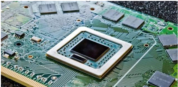
High speed backplane
2. Hardware configuration architecture design
① Function and total number of each dual board control module of system software
The overall data information exchange capacity of the system software determines the single slot data information volume of the business process sub card in the system software and the total number of business process sub cards;
The total number of other sub cards in the system software, such as the total number of key interchangeable sub cards, the total number of master chip sub cards, and the total number of switching power supply/cooling fan modules of the entire equipment.
② Model, specification and total number of socket connectors connecting each control module and backplane
Determine the actual model selection of interface connectors of each module according to the total number of signals
③ Frame design related to the whole equipment frame design
Sub card slot spacing, sub card structure oriented design plan, total power of system software switching power supply, system software heat pipe cooling air duct design, etc
3. Overall design plan
Generate the text document of the overall design plan of the backplane from the early important technical demonstration and the design plan of the hardware configuration architecture, and do the pre simulation analysis of the high-speed signal routing protocol
4. PINMAP design
This link has already entered the detailed design and completion of the backplane. Because the backplane has signal sockets in the product system and each hardware configuration function sub control module, it is necessary to define the definition method of all socket signals on the socket connector, similar to PINMAP integrated with ic pins
On the one hand, the backplane PINMAP design must focus on the crosstalk manipulation of high-speed interface signals (for example, one GND signal or two GND signals must be spaced between signals); On the other hand, you must pay attention to the completeness of PCB Layout design (generally, the backplane PCB routing must be smooth, and the number of stacked layers of high-speed backplane is generally high. If the signal definition is distorted, the number of stacked layers of PCB design will increase exponentially)
Circuit schematIC design
The circuit schematic design of the backplane is relatively simple, and can be made according to the self-developed tool software script to immediately convert PINMAP to circuit schematic
5. PCB design
It can be achieved in early work. Generally, the design of backplane PCB is completed without too much difficulty coefficient. It can be connected according to clear routing standards. The most important thing is to ensure the current carrying capacity of the power supply system of the system software switching power supply
6. UT detection
The backplane UT unit test volume focuses on the SI characteristics of the backplane high-speed signal security channel. At this time, the connector detection board will be used as a detection aid
7. System software integration test
The whole process of system software integration test will be long. Since the backplane itself and each hardware configuration sub control module have sockets, there will be many detection scenarios under different arrangements and combinations, such as communication between the exchange sub card and the business process sub card, communication between the master chip sub card and the business process sub card, and communication between the master chip sub card and the entire device sub control module.


抖音二维码

Q Q二维码

微信二维码
点击
然后
联系
然后
联系
电话热线
13410863085Q Q

微信

- 邮箱