鑫景福致力于满足“高品质”PCBA订购单需求。


Five Development Trends of PCB Technology in the 21st Century
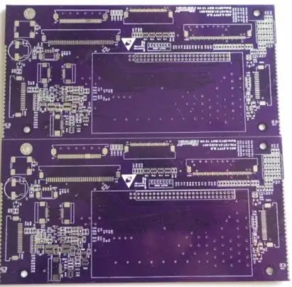
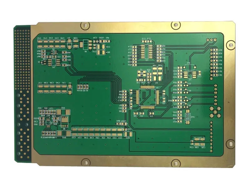
In the 21st century, human beings have entered a highly information society, and PCB is an indispensable pillar in the information industry. ElectronIC equipment requires high performance, high speed, light weight and miniaturization. As a multidisciplinary industry, PCB is the most critical technology of high-end electronic equipment. In PCB products, no matter rigid, flexible, rigid flex multilayer boards, as well as module substrates used for IC packaging substrates, have made great contributions to high-end electronic equipment. PCB industry plays an important role in electronic interconnection technology.
1、 Developing along the road of high-density interconnection technology (HDI)
As HDI embodies the most advanced technology of contemporary PCB, it brings fine wiring and micro aperture to PCB. Mobile phone (mobile phone), one of the electronic products of HDI multilayer board application terminal, is a model of HDI's cutting-edge development technology. In the mobile phone, the PCB main board fine wire (50 μ m~75 μ m/50 μ m~75 μ m. Conductor width/spacing) has become the mainstream, in addition, the thickness of conductive layer and plate is thin; The miniaturization of conductive patterns brings high-density and high-performance electronic equipment.
2、 Component embedding technology has strong vitality
The formation of semiconductor devices (calLED active components), electronIC components (called passive components) or passive component functions "component embedded PCB" in the inner layer of PCB has begun to be mass produced. Component embedded technology is a huge change in PCB functional integrated circuits, but to develop it must solve the SIMulation design method, and the production technology and inspection of quality and reliability assurance are urgent. We need to increase resource investment in systems including design, equipment, detection and simulation to maintain strong vitality.
3、 Material development in PCB should be further improved
Whether rigid PCB or flexible PCB materials, with the global lead-free electronic products, it is required that these materials must have higher heat resistance. Therefore, new types of high Tg, SMAll thermal expansion coefficient, small dielectric constant, and excellent dielectric loss tangent materials continue to emerge.
4、 Photoelectric PCB has broad prOSPects
It uses optical path layer and circuit layer to transmit signals. The key of this new technology is to make optical path layer (optical waveguide layer). It is an organic polymer formed by lithography, laser ablation, reactive ion etching and other methods. At present, the technology has been industrialized in Japan and the United States.
5、 manufacturing process shall be updated and advanced equipment shall be introduced
manufacturing process
HDI manufacturing has become mature and tends to be perfect. With the development of PCB technology, although the manufacturing methods commonly used in the past are still dominant, low-cost processes such as additive and sEMI additive have begun to emerge.
Using nanotechnology to metallize holes and form PCB conductive patterns at the same time, a new flexible board manufacturing process is developed.
High reliability, high quality printing method, ink-jet PCB technology.
Advanced equipment
Production of fine wires, new high-resolution photomask and exposure devices, and laser direct exposure devices.
Uniform coating equipment.


抖音二维码

Q Q二维码

微信二维码
点击
然后
联系
然后
联系
电话热线
13410863085Q Q

微信

- 邮箱