鑫景福致力于满足“高品质”PCBA订购单需求。


Common mistakes in designing custom PCB layout
Designing custom PCB layout usually brings challenges to complex electronIC projects A SIMple error, no matter how SMAll it looks, may cause the project to malfunction These common mistakes in PCB design may increase the manufacturing cost of customized PCB from the beginning
This article will explain 15 common mistakes you should know and avoid when designing custom PCB. Don't worry, even if you are new, even experienced engineers will make these mistakes. Avoiding them will mean high-quality products, reduce the production cost of customized PCBs, and there will be no manufacturing delay or rework requirements. Let's get started.
Regardless of available PCB design tools
Designers usually do not consider all available and easy to use custom PCB design tools. This is a serious mistake, because there are many design tools that can meet the various needs and flexibility requirements of PCB. You can use custom PCB design software to perform tasks such as scan design errors, component placement, and prototyping. The software is very cheap, based on the network, and even free access.
Narrow high current path
If your project has to deal with currents that are more important than a few hundred milliamperes, then a narrow PCB track width is not enough. Keep in mind that under the same thickness, the external PCB trace can carry higher current than the inner layer. The reason is that the former has more heat dissipation and airflow.
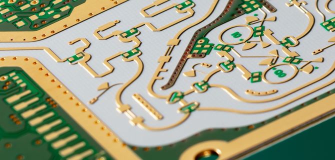
Circuit board

Many custom PCB manufacturers will provide you with copper weight options ranging from 0.5 oz/sf to 2.5 oz/sf. We suggest that you use the trajectory width small abacus to calculate its current carrying capacity.
Improper placement of decoupling capacitor
Decoupling capacitors in custom PCB design provide services for pins requiring stable and clean voltage. You can put them near the pins to get enough, calm energy. In addition, the power track of the power rail is also connected to the bolt through a decoupling capacitor. You can also make a series inductance low-pass filter to eliminate any input noise.
No optimized switch regulator layout
In electronic customized PCB design, there are two types of voltage regulators: linear voltage regulators and switching voltage regulators. Linear regulators are easy to arrange and cheap, but they waste a lot of power. However, deSPIte their complexity, switch regulators are very efficient because they consume very little energy. With them, your battery life will be longer. Recall that it is important to follow the data sheet guidelines in PCB layout.
Error drawing landing mode
The software used to customize PCB design provides libraries for components containing: PCB landing mode and schematic symbols If you only use library components, there will be no problem However, you need to manually draw the positioning pattern and legend of the part that does not exist Therefore, you need to be careful, because even if the pad spacing is only one mm, there will be welding and alignment problems
Unfabricated embedded hole or blind hole
If the budget is limited, we recommend that you do not use blind holes or embedded vias in PCB prototyping. The through-hole passes through all layers of the PCB, and they will definitely add the size of the PCB. However, they are cheaper than buried or blind vias. The embedded system is electrically connected with the two inner layers, and the blind hole connects the inner layer and the outer layer.
It is worth mentioning that this is not as easy as it sounds. When designing a custom PCB layout, you need to maintain the design constraints related to layer stacking.
Improper antenna layout
Antenna custom PCB layout is very important for electronic projects using wireless technology. Even electrical engineers sometimes make mistakes. You may need to match the complex impedance of the antenna and transceiver to achieve maximum power transmission. This requires a suitable transmission line.
For most antennas, a transmission line with an impedance of 50 ohms is sufficient to transmit the maximum power. You can use a free online abacus (such as AppCAD) to calculate the ratio of transmission lines. You can also place an LC pi network between the transceiver and the antenna to fine tune the antenna impedance.
Long high-speed routing
The straightest and shortest available path shall be used for high-speed signal. This will help if you point to any high-frequency crystals when designing your custom PCB correctly. Many microcontroller based PCB designs require only a few high-speed signals. However, if your project has high-speed microprocessors, address buses, and external data, you need to be vigilant.
No second opinion
Engineers usually work within tight deadlines and focus on getting results from custom PCB production. This causes a custom PCB design error. It is better to have another bit engineer review your PCB design to avoid the high cost of customized PCB production. The rule is simple: if errors are found later, they will become more expensive.
Large skater
Talc is an insoluble copper in chEMIcal etching process. It seems that these are connected to PCB and customized PCB manufacturing appearance, which may also cause short circuit. This will help if you ensure that the minimum copper width is greater than that required by the custom PCB manufacturer. In this way, the coasting will be reduced and the PCB will work normally.
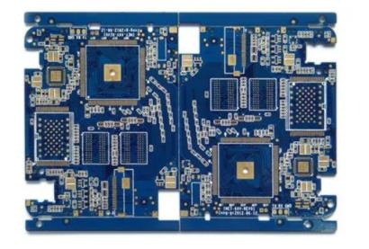
Complex custom PCB design
Customized PCB manufacturers can produce PCBs more efficiently and economically if they understand their basic working principles. However, if the design is complex, problems such as unbalanced schematics may arise. Recall that you must try to simplify the custom PCB design to avoid any design errors. In addition, this will improve the effectiveness of the design.
Using incorrect components or custom PCB layout methods
What is needed now is to design complex custom PCB layouts using smaller components and smaller footprint. To this end, designers use ball grid array packaging and embedded devices in the inner layer of PCB. It helps improve project performance and allows rework in the event of any errors.
For components with small spacing and high number of pins, the correct layout method must be selected. Doing so during the design phase will save you the cost of custom PCB production. In addition, if you plan to use replacement components, be sure to check whether their performance characteristics match the original components, so as to avoid abandoning the customized PCB design in the later stage.
Forgot to save all PCB design files when customizing PCB layout
Always back up custom PCB design files. If your software does not respond initially, the file may be lost. Do not save it until the entire design is completed. You should at least store files that are difficult to retrieve. Most custom PCB manufacturers provide daily backups, but smaller companies may not provide such facilities. Besides, if you work alone at home, this is impossible.
Nowadays, with the emergence of "cloud" services, there is no reason to safely back up PCB design files. If you plan to mass produce products or want to put them on the MARKet, this will also ensure that your custom PCB design is protected from fire, counterfeiting, threats, malware and other technological disasters.
Do not consult the custom PCB manufacturer in advance
Custom PCB manufacturers usually follow their registered production processes to improve the efficiency of their employees and equipment. If you don't pay attention to their manufacturing methods, your project costs may rise or manufacturing delays may occur. You will also waste time because you need to contact other custom PCB manufacturers. In addition, you may need to redesign the custom PCB layout according to the manufacturer's specifications.
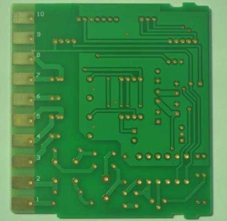
Custom PCB layout does not need to test custom PCB
Once you have made a custom PCB Prototype, you should thoroughly check it It shall be ensured that the initial operation requirements of the design are met In addition, you can also test environmental conditions that may affect PCB stability or reliability This is to ensure extensive operation of custom PCB if you don't do this, your custom PCB prototype may fail when it is finally released to the market
PCB leaders welcome growth opportunities
11-13,2022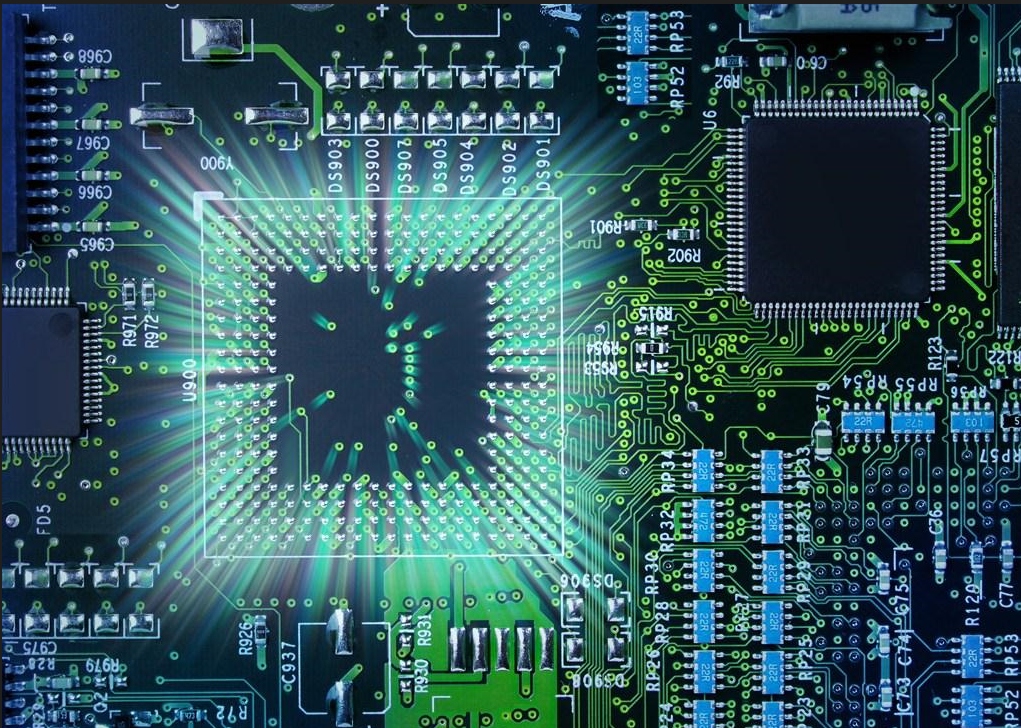


抖音二维码

Q Q二维码

微信二维码
点击
然后
联系
然后
联系
电话热线
13410863085Q Q

微信

- 邮箱