鑫景福致力于满足“高品质”PCBA订购单需求。


Etching Technology of PCB External Circuit
At present, the typICal process of PCB processing is "pattern electroplating" That is, a lead tin resistance layer is pre plated on the copper foil to keep it on the outer layer of the board. That is, the graphic part of the circuit is then chEMIcally etched off the remaining copper foil, which is calLED etching In terms of etching process, it should be noted that there are two layers of copper on the circuit board at this time In the outer etching process, only one layer of copper must be completely etched, and the rest will form the final required circuit This pattern plating is characterized by the presence of a copper layer only under the lead tin resist Another process is to plate copper on the whole circuit board, and the parts other than the photosensitive film are only tin or lead tin corrosion resistant layers This process is called "full plate copper plating process" Compared with pattern electroplating, the disadvantage of full plate copper plating is that copper must be plated twice anywhere on the plate and must be etched during etching Therefore, when the wire width is very thin, a series of problems will occur At the same time, side corrosion will seriously affect the uniformity of the pipeline Tin or lead tin is a common resist layer used in the amino etchant etching process Ammonia etchant is a common chemical liquid, which has no chemical reaction with tin or lead tin Ammonia etchant mainly refers to ammonia/ammonium chloride etchant In addition, ammonia/ammonia sulfate etching solution is also available on the MARKet After use, the copper in sulfate corrosion solution can be separated by electrolysis and reused Due to its low corrosion rate, it is rarely seen in practical production, but it is expected to be used for chlorine free etching Some people tried to use hydrogen sulfate as an etchant to etch the outer pattern For many reasons, including the economy and waste treatment, this process has not been adopted commercially In addition, sulfuric acid hydrogen peroxide cannot be used for the etching of lead tin resistance, and this process is not the main method to produce the outer layer of PCB, so most people pay little attention to it
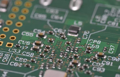
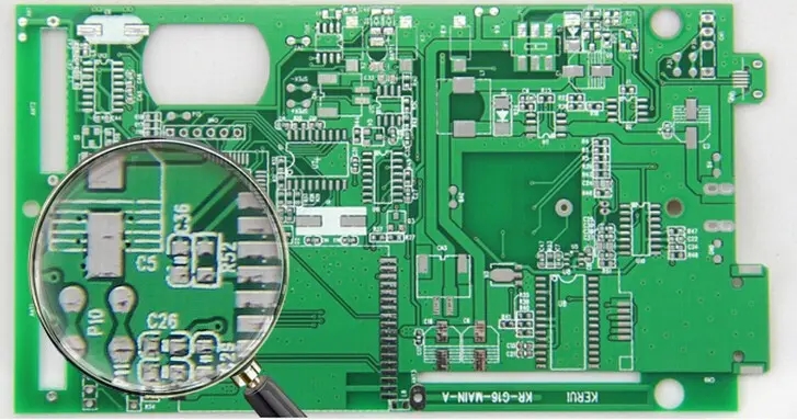
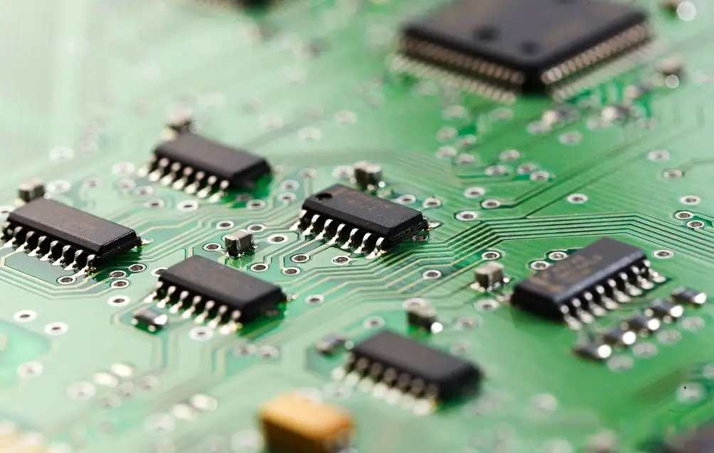
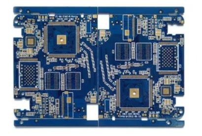
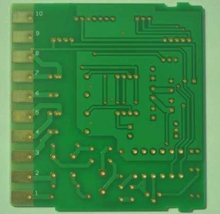
Printed circuit board

1. Etching quality and early problems
The basic requirement for getting quality is to be able to completely remove all partner layers except under the existing layer Strictly speaking, if the grounding is to be defined, the etching quality must include the uniformity of line width and the degree of side etching Due to the inherent characteristics of current etchants, they not only etch downward, but also etch left and right, so side etching is almost inevitable Undercut is one of the etching parameters often discussed It is defined as the ratio of undercut width to etching depth, called etching factor In the printed circuit industry, the difference is very large, from 1:1 to 1:5. Obviously, SMAller undercut degree or lower etching coefficient is satisfactory The structure of the etching equipment and the different components of the etching solution will affect the etching factor or the side etching scale, or optimistically, it can be controlled The use of certain additives can reduce the degree of side etching The chemical composition of these additives is usually a trade secret, and their developers will not disclose it to the outside world As for the structure of etching equipment, the following chapters will introduce it professionally
In many ways, the etching quality is as early as the PCB enters the etcher Because each process of printed circuit processing has a very close internal relationship, there is no process that is not affected by other processes and does not affect other processes Many problems identified as etching quality actually existed even earlier in the stripping process It is used for the etching process of the outer pattern. It reflects many problems, because it reflects the "countercurrent" phenomenon more prominent than most PCB processes At the same time, this is also because etching is part of a series of processes starting from the mucous membrane and the photosensitive film, after which the outer pattern is successfully transferred The more connections you have, the more likely you are to have problems This can be regarded as a very special aspect of the printed circuit production process
Theoretically, after the printed circuit enters the etching stage, in the process of processing the printed circuit with pattern electroplating, the ideal state should be: the sum of the thickness of copper and tin or copper and lead tin after electroplating should not exceed the thickness of the photosensitive film of the electroplating resistor, so that the electroplating pattern is completely blocked by the "walls" on both sides of the film and embedded in it However, in actual production, the coating pattern of electroplated PCB is much thicker than the photosensitive pattern all over the world In the process of electroplating copper and lead tin, because the height of the electroplating layer is higher than that of the photographic film, there is a trend of horizontal accumulation, and the problem arises The tin or lead tin anti-corrosive layer covering the upper part of the strip extends to both sides to form an "edge", and a small part of the photosensitive film is covered under the "edge" The "edge" formed by tin or lead tin makes it impossible to completely remove the film when removing it, leaving a small part of "residual glue" under the "edge" "Residual adhesive" or "residual film" left below the "edge" of the resist will result in incomplete etching After etching, the lines form a "copper root" on both sides, which narrows the line spacing, resulting in the printed circuit board not meeting the requirements of Party A, or even being rejected Production cost PCB will be greatly increased due to rejection In addition, in many cases, due to the formation and dissolution of reaction, in the printed circuit industry, the residual film and copper may also form deposits in the etching solution and block the nozzles of the etcher and acid resistant pump, so they must be closed for treatment and cleaning, Affect work efficiency
2. Equipment adjustment and interaction with corrosive solution
In printed circuit processing, ammonia etching is a relatively fine and complex chemical reaction process Conversely, it is an easy job Once the process is started, production can continue The key is that once it is started, it needs to keep working continuously. It is not recommended to stop The etching process depends to a large extent on the good working conditions of the equipment At present, no matter what kind of etching solution is used, high-pressure spraying must be used. In order to obtain neat line edges and high-quality etching effect, the nozzle structure and spraying method must be strictly selected In order to obtain good side effects, many different theories have emerged, leading to different design methods and equipment structures These theories are usually very different However, all etching theories recognize the basic principle of keeping metal surfaces in constant contact with fresh etchants as quickly as possible The chemical mechanism analysis of the etching process also confirmed the above viewpoint In ammonia etching, assuming all other parameters remain unchanged, the etching rate is mainly determined by the ammonia in the etching solution Therefore, there are two main purposes for etching the surface with fresh solution: one is to wash the newly generated copper ions; The other is to continuously supply ammonia for reaction
Traditional knowledge of the printed circuit industry, especially the suppliers of printed circuit raw materials, generally believes that the lower the content of monovalent copper ions in the amino etching solution, the faster the reaction speed This has been proved by experience In fact, many ammonia based exchange products contain special ligands (some complex solutions) for monovalent copper ions, which act to reduce monovalent copper ions (these are the technical secrets of their products' high reactivity) By reducing the unit price of copper from 5000 ppm to 50 ppm, the etching rate will be more than doubled Because a large number of monovalent copper ions will be generated during the etching reaction, because monovalent copper ions are always closely bound with the complex groups of ammonia, it is difficult to keep the content close to zero The monovalent copper can be removed by converting monovalent copper into bivalent copper through the action of oxygen in the atmOSPhere This can be achieved by spraying This is a functional reason for allowing air to enter the etching chamber However, if there is too much air, it will accelerate the loss of ammonia in the solution and reduce the pH value, which will still reduce the etching rate Ammonia in solution is also a variable to be controlled Some users adopt the method of passing pure ammonia into the etching tank To do this, a PH meter control system must be added When the automatically measured pH value is lower than the given value, the solution will be added automatically In the related field of chemical etching (also known as photochemical etching or PCH), the research work has begun and has reached the structural design stage of the etching machine In this method, the solution used is bivalent copper, not ammonia copper etching It is likely to be used in the printed circuit industry In the PCH industry, etched copper foil is usually 5 to 10 mils thick, and in some cases is quite thick Its requirements for etching parameters are generally stricter than those of PCB industry
3. the problem of different setting states between the lead in edge and the rear entry edge
A large number of problems related to etching quality are concentrated on the etched part of the upper board surface. It is important to understand this These problems stem from the colloidal accumulation effect of etchants on the surface of printed circuit boards Colloidal solids accumulate on the copper surface, which will affect the ejection force on the one hand, and hinder the supplement of fresh etching solution on the other hand, resulting in a decrease in etching rate It is due to the formation and accumulation of colloidal solids that the upper and lower patterns of the circuit board are etched differently This also makes the part of the circuit board that first enters the etching machine easy to be completely etched or easy to cause excessive corrosion, because there is no accumulation at that time, and the etching speed is faster On the contrary, when the part entering the back of the plate enters, the deposit has formed and slows down its etching rate
4. The maintenance of etching equipment
The key factor in the maintenance of etching equipment is to ensure that the nozzles are clean and free of obstructions to make the spraying smooth. Clogging or slagging will affect the layout under jet pressure If the nozzle is not clean, the etching will be uneven and the entire PCB will be discarded Obviously, the maintenance of the equipment is to replace damaged and worn parts, including the replacement of nozzles In addition, the more critical problem is to keep the etcher free of slag accumulation, which can happen in many cases Excessive slag accumulation may even affect the chemical balance of etching solution SIMilarly, if the etchant exhibits excessive chemical imbalance, the formation of slag will intensify The problem of slag accumulation cannot be overemphasized Once a large amount of slagging suddenly appears in the etching solution, this is usually a signal indicating that there is a problem with the balance of the solution A stronger hydrochloric acid shall be used for proper cleaning, or the solution shall be supplemented The residual film will also produce slag, and a small amount of residual film will be dissolved in the etching solution, and then copper salt precipitation will be formed The slag formed by the residual membrane indicates that the previous membrane removal process is incomplete Poor film removal is usually edge film and PCB creeping plating

抖音二维码

Q Q二维码

微信二维码
点击
然后
联系
然后
联系
电话热线
13410863085Q Q

微信

- 邮箱