鑫景福致力于满足“高品质”PCBA订购单需求。


Important factors to be considered by PCBA designers
The definition of PCBA's overall design scheme for processing and manufacturing is briefly stated. I hope it can help you to some extent. It clarifies PCBA's design scheme for manufacturability, whICh mainly includes the following four design scheme factors.
1. Automatic assembly line double plate transmission and precise positioning factor design scheme Automatic assembly line, PCBA processing must have the working ability of transmission edge and electronic optical precise positioning MARK, which is a prerequisite for manufacturing.
2. PCBA processing and assembly step design scheme
The design scheme of PCBA processing and assembly steps, that is, the reasonable layout and structure of Electronic devices on both sides of PCB. It determines the processing method and relative path during assembly, so it is also calLED the relative path design scheme of processing technology.
3. Reasonable layout design scheme of PCBA processing electronic devices
The reasonable layout design scheme of electronic devices, namely, the design scheme of the position, orientation and spacing of electronic devices on the surface of the assembly line. The reasonable layout of electronic devices depends on the selected welding process. Each welding process often has special provisions on the distribution position, orientation and spacing of electronic devices. Therefore, this book introduces the reasonable layout design scheme in detail according to the welding method selected for packaging. It must be emphasized that sometimes two or more welding methods can be selected for one assembly line, such as "reflow welding plus wave peak welding". In this case, a reasonable layout design scheme should be developed according to the welding method selected for each package.
4. PCBA processing and assembly process performance design scheme
The assembly process performance design scheme, i.e. the design scheme towards the welding straightness rate of electric welding, shall be based on the matching design scheme of through-hole, solder mask and screen plate to maintain the quantitative analysis of solder paste and the specified stable distribution; According to the design scheme of reasonable layout and routing, keep the SIMultaneous melting and condensation of all spot welding separately packaged; According to the effective wiring design scheme of the mounting hole, the tin penetration rate of 75% is maintained. The overall goal of this design scheme is to improve the qualification rate of electric welding.
For example, the through-hole design scheme of 0.4mmCSP on the mobile phone upper plate of Kyocera Corporation of Japan selects the design scheme of resistance welding defining through-hole, which aims to improve the qualification rate of electric welding. Such a design scheme, on the one hand, creates a solder mask plan, which is beneficial to the sealing between the screen board and PCB; On the other hand, it improves the amount of solder paste and reduces the risk of ball and socket caused by insufficient total output of solder paste.
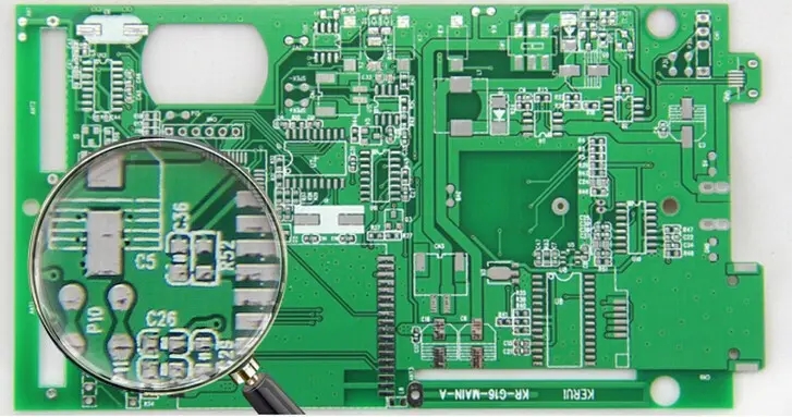
PCB manufacturers, PCB designers and PCBA manufacturers will explain some important factors that PCBA Designers need to consider.


抖音二维码

Q Q二维码

微信二维码
点击
然后
联系
然后
联系
电话热线
13410863085Q Q

微信

- 邮箱